Intelligence BuildoutMethodology

Package — complete text edition

Volume III / Text edition

Package

Advanced packaging + memory. 14 spreads and 28 pages, with the complete evidence-linked content. No JavaScript is required.

Volume III

Package

Advanced packaging + memory · 28 pages

Where finished dies become a tightly coupled compute system—and where memory bandwidth, assembly yield, thermal paths, and substrate capacity decide how much silicon becomes useful intelligence.

01

The system moves onto the package

Advanced packaging is architecture, interconnect, power delivery, mechanics, and manufacturing compressed into one assembly.

Spread 01 / A new system boundary

01 / System boundary

A package is no longer a protective shell

Modern AI silicon is assembled as a local system before it ever reaches a server board.

Traditional descriptions place packaging after fabrication, as though the difficult work ends when a good die leaves the wafer. AI accelerators overturn that sequence. Logic dies, memory stacks, passive structures, power-delivery paths, and high-density links must be integrated at distances short enough to move enormous volumes of data without the energy and latency penalties of a conventional board trace.

That makes the package an architectural boundary. Decisions about die partitioning, memory placement, interposer size, substrate routing, bump pitch, and heat removal constrain the accelerator long before a rack designer chooses a chassis. A brilliant die that cannot be assembled, powered, cooled, tested, or produced at acceptable yield is not deployable compute; it is unfinished inventory.

Read the stack
Die
A tested piece of patterned semiconductor cut from a wafer.
Package
The electrical, mechanical, and thermal assembly that makes one or more dies usable by a system.
Module
A packaged device plus the board, connectors, and local components needed for integration.
Three envelopes must agree
Design envelope
Die area, edge length, routing demand, power delivery, thermal paths, and protocol boundaries that the architecture requires.
Manufacturing envelope
Available substrate formats, alignment capability, material controls, inspection coverage, qualified tools, and recoverable yield at each assembly stage.
Operating envelope
Temperatures, currents, workload duty cycles, repair policies, and error rates within which the completed package must remain dependable.
The useful unit is the tested assembly, not the fabricated die alone.

Field plate / Integration

Physical proximity becomes performance

Dense interconnect lets logic and memory behave more like one machine, but every added interface creates another manufacturing obligation.

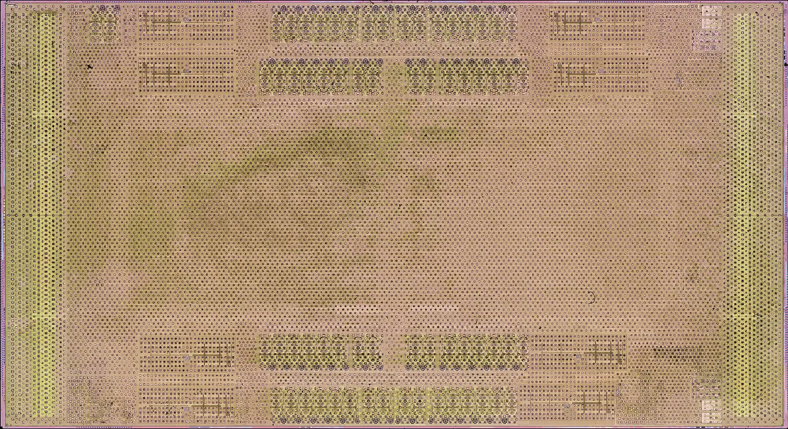
An advanced package shortens critical paths by moving components from separate board sockets onto a common integration structure. Thousands of fine connections can carry data and control signals while larger structures distribute power and provide mechanical support. The reward is bandwidth and integration density. The cost is tighter tolerances, more coupled failure modes, and an assembly flow that must protect components already carrying substantial embedded value.

The macrograph is best read as evidence of the physicality of microelectronic integration: dense patterned conductors must be fabricated and inspected across a real silicon surface. It is not a diagram of a current commercial AI product. Commercial packages vary by vendor and generation, yet all must solve the same basic problem—join fragile, dissimilar parts so that electrical, thermal, and mechanical behavior remains stable in production.

Highly magnified top metal of a silicon interposer with dense copper routing patterns.

A magnified silicon-interposer metal layer makes the dense physical routing beneath logic and memory visible.

Historical component macrograph; it does not depict a current CoWoS production line or disclose a current AI package design.The creator waived copyright and related rights under CC0. Credit is retained as editorial provenance.Fritzchens Fritz / Wikimedia Commons, CC0.Original sourceCC0 1.0 Universal
Questions before choosing proximity
  • Which traffic actually benefits from shorter traces, and which traffic can tolerate board- or rack-scale distance?
  • What new heat density, routing congestion, power-delivery impedance, or inspection blind spot is created by moving components closer?
  • Can every high-value element be tested before integration, and can the finished assembly isolate or tolerate a partial defect?
Integration density trades board distance for package complexity.

Spread 02 / Chiplets and partitioning

02 / Partition

One product, many dies

Chiplets let designers divide a large system into manufacturable pieces and mix functions made on different processes.

A monolithic die keeps communication on one piece of silicon, but die area, defect exposure, reticle limits, and process cost can make ever-larger designs difficult to manufacture. Chiplet architectures divide the system: compute tiles, input/output functions, cache, interface dies, or other blocks can be fabricated separately and then joined within the package. Each block can use a process suited to its function rather than forcing every transistor onto the most advanced node.

Partitioning is not free modularity. Interfaces consume edge area and power; protocol and clock boundaries add design work; and the package must provide enough wires with predictable latency. Teams also need test strategies for each die before assembly and system-level validation afterward. The economic benefit therefore depends on co-design across architecture, physical design, fabrication, packaging, and software—not on simply cutting one schematic into smaller rectangles.

Partition choices move constraints rather than removing them
ChoicePotential advantageTransferred burden
MonolithicShortest on-die pathsLarge-die yield and process cost
Homogeneous chipletsRepeatable tilesDie-to-die fabric and assembly
Heterogeneous chipletsProcess matched to functionQualification and interface governance
Partition from workload to package
  1. Map traffic— Quantify bandwidth, latency sensitivity, coherence, clocking, and burst behavior before drawing die boundaries.
  2. Price the seam— Budget shoreline, PHY power, protocol overhead, repair logic, package routes, and verification effort for every cut.
  3. Prove composition— Validate die identity, initialization order, fault containment, security roots, and system behavior across supported combinations.
Chiplets redistribute complexity from the wafer into interfaces and assembly.

Architecture / Co-design

The seam becomes a design object

Every die-to-die boundary needs a physical channel, protocol, power budget, test plan, and failure model.

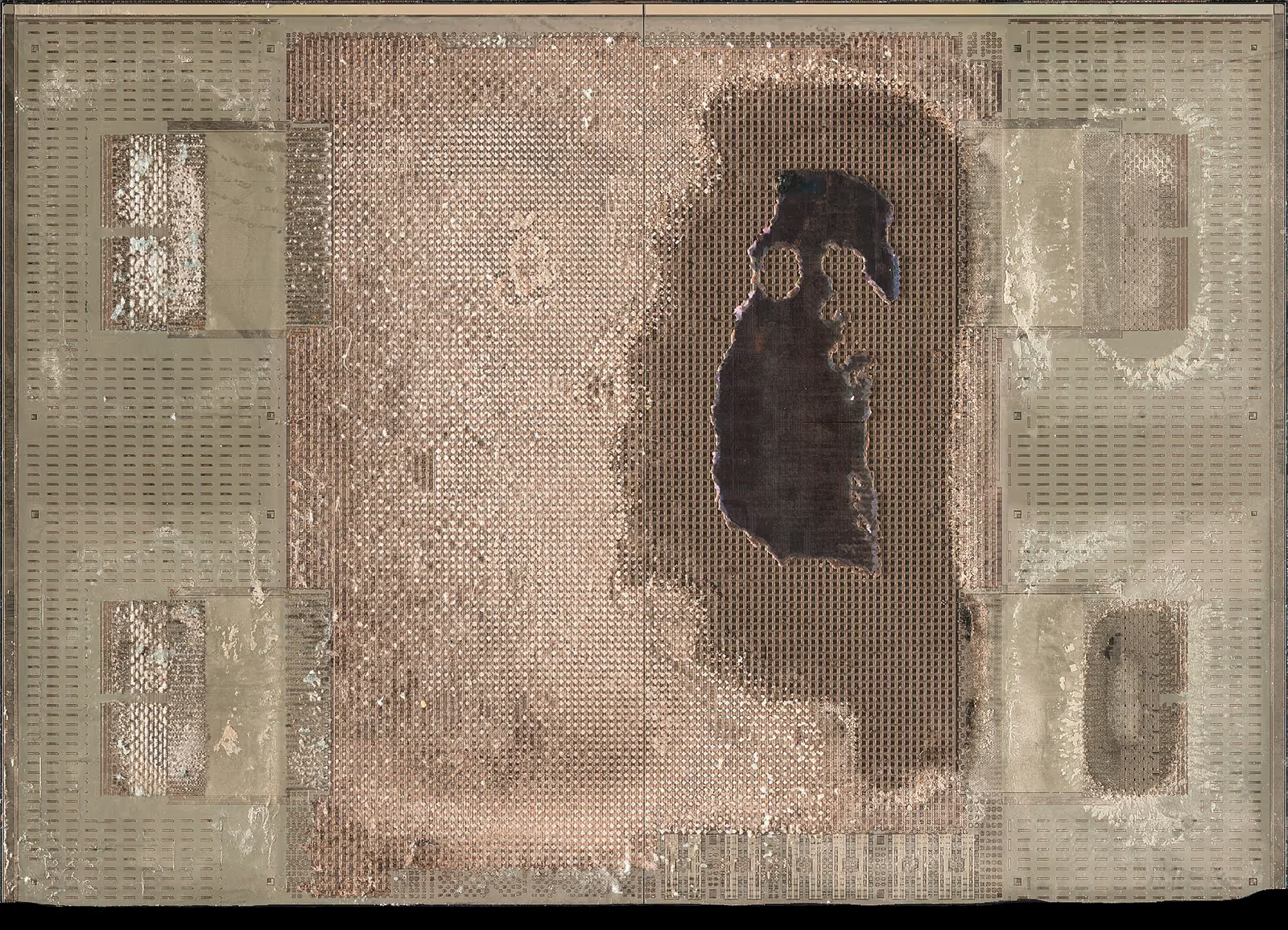
Inside a chiplet product, the seam is where multiple disciplines meet. Circuit designers shape transmitters and receivers; package engineers route dense channels; mechanical engineers manage warpage; firmware discovers and initializes components; and software must understand the topology well enough to place work efficiently. A boundary that looks clean in an architectural diagram may become congested when routing escapes, power delivery, and thermal keep-out zones are added.

This is why standards and reusable interfaces matter, but standards alone do not make chiplets interchangeable. Known-good-die requirements, security roots, repair behavior, coherent memory semantics, and vendor qualification still determine whether two components can share a package. The macrograph shows one historical server-processor input/output die, making a separately fabricated function tangible. It should not be read as a map of a current AI accelerator or as evidence that all chiplets use the same integration method.

Magnified top metal of an exposed server-processor I/O die showing patterned functional regions.

A macrograph of one historical server-processor I/O die makes the physical reality of a separately fabricated system function visible.

Historical implementation, not a current AI accelerator floorplan or a claim of cross-vendor chiplet interchangeability.The creator waived copyright and related rights under CC0. The image documents one historical implementation, not a universal chiplet layout.Fritzchens Fritz / Wikimedia Commons, CC0.Original sourceCC0 1.0 Universal

UCIe specifies a die-to-die interface, but a published rate is only the signaling ceiling for a compliant option. Real bandwidth depends on lane count, coding and protocol overhead, package reach, error handling, and the product's implemented profile. Interoperability still requires compliance testing plus shared assumptions about discovery, firmware, reset, security, and lifecycle management; the chart therefore reports specification options, not achieved multi-vendor throughput.Claim

UCIe documented maximum transfer-rate options

Published per-lane transfer-rate ceilings for UCIe 2.0 and the two higher-rate options introduced by UCIe 3.0.
Maximum specified rateGT/s
View chart values
UCIe documented maximum transfer-rate options — underlying values in GT/s
CategoryMaximum specified rate
UCIe 2.032 GT/s
UCIe 3.0 option48 GT/s
UCIe 3.0 option64 GT/s

SPECIFICATION OPTIONS — not measured payload bandwidth, product availability, compliance, or demonstrated cross-vendor interoperability.

A chiplet boundary is electrical, mechanical, logical, and contractual at once.

Spread 03 / Interposers, redistribution, and substrates

03 / Routing

Different layers solve different distances

Fine-pitch connections near the dies must eventually fan out into the coarser geometry of a server board.

The package is a hierarchy of routing scales. Micro-bumps or direct bonds connect dies to a nearby structure. Redistribution layers rearrange connection patterns. A silicon interposer or bridge can carry very dense die-to-die and memory links. Beneath that, an organic substrate fans signals and power outward to solder balls or other board-level contacts. Each transition changes conductor geometry, dielectric material, manufacturing process, and the defects engineers must control.

For AI products, routing is consumed quickly by wide memory interfaces, scale-up links, clocks, management signals, and power delivery. More wiring area is not automatically better: larger structures may worsen cost, warpage, yield exposure, and lithographic requirements. Designers therefore balance interposer extent, bridge placement, layer count, escape routing, and the location of decoupling components. The result is a spatial negotiation among bandwidth, power integrity, manufacturability, and cooling access.

From die pad to board
  1. Join— Create fine-pitch die connections by bumps or bonding.
  2. Redistribute— Re-map dense interfaces across metal layers.
  3. Fan out— Move signals and power into substrate-scale geometry.
  4. Land— Connect the completed package to the module board.
Routing layers solve different physical problems
LayerPrimary jobDecision boundary
Local bridgeDense die-edge connectionLimited reach and placement freedom
Silicon interposerFine, broad package routingArea, cost, stress, and process complexity
RDL structureFan-out and redistributionLayer count, line geometry, and warpage
Package substrateEscape to board and powerVia density, materials, yield, and availability
Routing density must taper from microscopic die interfaces to serviceable boards.

Materials / Interfaces

Every layer expands the bill of materials

Silicon, copper, polymers, solder, underfill, adhesives, and thermal materials must survive one another.

Advanced integration combines materials with different coefficients of thermal expansion, stiffness, surface chemistry, and moisture behavior. Heating during assembly and later operation makes those differences physical: structures bow, joints fatigue, interfaces delaminate, and resistance can drift. Underfill supports fine connections; molding compounds protect components; substrate laminates carry routing; and thermal-interface materials bridge imperfect surfaces. None is merely packaging consumable—the selected formulation changes reliability and process windows.

Supply resilience must therefore be tracked at formulation and qualified-part level, not just by counting substrate factories. A replacement resin, copper foil, solder composition, or bonding film may require reliability testing and customer approval even when it appears functionally similar. The package turns a materials catalog into a coupled stack. That coupling is why bottlenecks can persist after headline capacity expands: new lines still need qualified chemistry, tooling, inspection recipes, and stable yields.

Four coupled behaviors
  • Electrical: loss, crosstalk, resistance, and power integrity
  • Thermal: heat spreading, interface resistance, and hotspots
  • Mechanical: warpage, stress, shock, and fatigue
  • Chemical: adhesion, corrosion, contamination, and moisture uptake
Material interfaces to audit
  • Coefficient-of-expansion mismatch can bow the assembly during cure, reflow, thermal cycling, or operation and shift joint stress elsewhere.
  • Moisture, contamination, surface roughness, and incomplete underfill can turn an electrically correct layout into a latent reliability problem.
  • Power planes, high-speed routes, thermal paths, and mechanical keep-outs compete for the same area; optimizing one layer can constrict another.
Qualification attaches to a material stack, not to a generic label.
02

Memory beside compute

HBM changes the geometry of memory access, while DRAM, NAND, and storage remain a hierarchy rather than substitutes.

Spread 04 / The memory hierarchy

04 / Hierarchy

Compute waits at every distance

AI performance depends on moving the right bytes through a hierarchy of capacities, bandwidths, latencies, and persistence.

Registers and on-die caches are extremely close to arithmetic but limited in capacity. High-bandwidth memory sits beside the accelerator package and supplies wide, parallel access. Host DRAM provides a larger pool across an interconnect. Local SSDs, shared flash, and networked storage hold datasets and checkpoints with progressively different latency and persistence. No single layer replaces the others because each occupies a distinct cost, capacity, energy, and distance envelope.

The engineering objective is not simply to buy faster memory. Models, batch sizes, precision formats, attention caches, optimizer state, and parallelism determine where capacity pressure appears. Software then must stage and reuse data so expensive arithmetic units remain occupied. When working sets spill to a slower tier, the accelerator can become a waiting device. Packaging matters because it makes the fastest external memory tier physically adjacent to logic.

A functional—not vendor-specific—memory hierarchy
TierPrimary valuePrimary limit
On-die cacheLowest local latencyVery limited capacity
HBMVery wide package-level bandwidthStack capacity and heat
Host DRAMLarger working memoryInterconnect distance
SSD / shared storagePersistent scaleLatency and ingest throughput
Residency is an operating policy
Working set
The model state, activations, caches, buffers, and runtime data that must remain quickly reachable during a workload phase.
Reuse distance
The work performed between accesses to the same data, which helps determine whether a nearer cache or memory tier can retain it.
Movement penalty
Latency, energy, link occupancy, synchronization, and software overhead paid when data crosses a hierarchy boundary.
Memory is a choreography of tiers, not one specification.

Workload / Data motion

Bandwidth is useful only when software can consume it

A headline transfer rate describes an interface ceiling, not sustained application performance.

Memory bandwidth becomes productive when kernels issue enough concurrent work, access patterns align with the hierarchy, and data can be reused before eviction. Irregular access, synchronization, small transfers, poor layout, or insufficient parallelism can leave theoretical bandwidth untouched. Capacity also matters: a larger working set may reduce transfers across slower links even if the peak rate is unchanged. The right comparison is therefore workload-specific and measured across the full system.

This distinction is crucial for infrastructure planning. A memory-limited workload may gain more from capacity, bandwidth, or software changes than from additional arithmetic. Conversely, more HBM can increase package area, component count, assembly complexity, power, and heat. Architects choose an operating point rather than maximizing one metric. The package is where that choice becomes fixed in silicon, stacks, routing channels, and cooling geometry.

Measurement boundary: Vendor bandwidth is a component specification. Sustained model throughput also depends on kernels, access locality, interconnects, synchronization, and thermal behavior.

A hierarchy should be evaluated with traces, not capacity labels alone. Record where bytes originate, how often they are reused, whether transfers overlap computation, and which queue stalls the critical path. Cache-hit rate can improve while elapsed time worsens if placement adds synchronization or fragments batches. Report effective bandwidth, latency distribution, eviction traffic, and accelerator idle time at the same workload phase so a local optimization cannot hide a downstream penalty.

Peak bandwidth is an input to performance, not a performance result.

Spread 05 / How HBM is assembled

05 / Vertical memory

A stack is a manufactured structure

HBM places multiple thinned DRAM dies above a base interface and connects them through the silicon.

High-bandwidth memory gains its characteristic width by arranging many channels close to the accelerator and stacking memory dies vertically. Through-silicon vias carry signals through thinned dies; fine connections join layers; and a base die or interface layer coordinates communication with the package. The stack must be fabricated, thinned, aligned, bonded, inspected, and tested while protecting extremely small structures from particles, stress, and handling damage.

Adding stack height can increase capacity, but it also extends the assembly and thermal problem. Every additional die and interface contributes potential defects, resistance, and heat. The package designer must reserve edge length and routing for wide interfaces, while the memory supplier must control die thickness, via quality, bonding, and test. HBM capacity is thus inseparable from memory-fab output, stacking capacity, package capacity, and the yield of the combined flow.

Simplified HBM flow
  1. Fabricate— Create DRAM and interface dies with vertical connections.
  2. Thin— Reduce die thickness while preserving mechanical integrity.
  3. Stack— Align and bond dies through fine vertical interfaces.
  4. Integrate— Place tested stacks beside logic on the package.
Reliability follows the stack
  1. Qualify dies— Screen DRAM and interface dies before thinning and before additional value is attached.
  2. Control geometry— Hold thickness, alignment, coplanarity, via exposure, and surface condition inside the bonding window.
  3. Stabilize interfaces— Manage underfill or mold flow, cure, voids, stack pressure, warpage, and thermal expansion.
  4. Exercise the stack— Test electrical paths and thermal behavior before and after package-level environmental stress under representative duty cycles.
HBM is memory fabrication plus precision vertical assembly.

Field plate / Memory

Nearness is engineered, not abstract

The physical stack and its package connections are what turn a wide logical interface into an operable component.

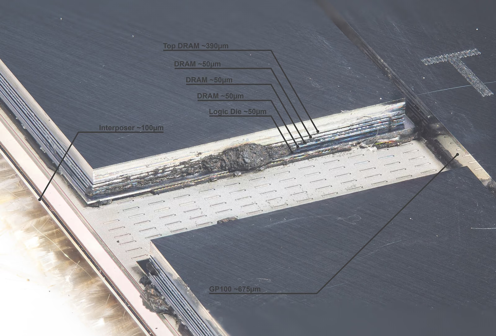
Photographs of memory hardware reveal a fact that block diagrams hide: bandwidth depends on surfaces, joints, conductors, and tolerances. A stack must remain flat enough to bond, intact enough to handle, and electrically uniform across a wide interface. Inspection and test have to find faults early because a failed component can strand other high-value parts after final integration. The assembly sequence is therefore designed around risk as much as throughput.

The image shown here documents a real memory or advanced-integration artifact identified in its source record. It provides physical context, not a teardown of the HBM configuration cited elsewhere in this volume. Product generations differ in die count, capacity, interface, and construction. The durable lesson is the dependency: accelerator availability can be limited by the least available qualified element among logic, HBM, integration capacity, substrates, and test.

Annotated macrograph identifying memory dies and logic in an HBM stack beside a processor.

Documentary memory hardware grounds the abstract idea of bandwidth in fabricated, handled, and tested physical components.

The pictured artifact is contextual; do not infer that it is the exact commercial HBM3E configuration used in cited accelerator specifications.The creator waived copyright and related rights under CC0. Labels belong to the original image.Fritzchens Fritz / Wikimedia Commons, CC0.Original sourceCC0 1.0 Universal
HBM evidence must locate the failure layer
ObservationPossible layerNext evidence
Intermittent lane errorsVertical or package linkPer-channel counters and stress retest
Temperature-correlated faultsStack, interface, or cooling pathThermal map and controlled load sweep
Capacity unavailableDie, stack, or controller policyConfiguration, repair state, and memory test
Early-life escapeAssembly or screening gapLot genealogy and destructive analysis
The widest interface still depends on tiny, repeatable physical joints.

Spread 06 / Capacity and bandwidth

06 / Product envelope

Capacity changes what can remain local

More package memory can reduce off-device transfers, but usable capacity is allocated across model state, activations, caches, and runtime overhead.

An accelerator’s HBM is not a single undifferentiated pool available to the model. Parameters, activations, gradients, optimizer states, attention caches, communication buffers, compiled kernels, and error-correction overhead compete for space depending on whether the workload is training or inference. Software may shard tensors across devices, recompute intermediates, offload data, or reduce numerical precision to fit within the available envelope.

Capacity therefore affects system topology and operating cost. If a workload fits on fewer devices, it may avoid communication and coordination; if it does not, the cluster must distribute state across links and accept additional failure and scheduling complexity. Yet larger memory configurations also demand more stacks, package area, assembly steps, and cooling. The specification is best understood as one boundary in a broader model-to-machine mapping exercise.

HBM3E capacity specified for NVIDIA H200
141 GB
Evidence class
vendor_spec
Claim
claim-h200-memory
Context
A product specification, not the memory available to every workload after system and software overhead.

The comparison records two stack capacities, not a benchmark. The parts differ in generation, height, supplier, interface, and status. Micron's 24 GB is an HBM3E eight-high specification; SK hynix's 36 GB described a twelve-high HBM4 sample. Capacity alone does not establish qualification, availability, yield, bandwidth, thermals, price, or delivered performance.ClaimClaim

Documented capacity for two unlike HBM configurations

Capacity per stack for a Micron HBM3E eight-high specification and an SK hynix HBM4 twelve-high customer sample.
Documented capacityGB per stack
View chart values
Documented capacity for two unlike HBM configurations — underlying values in GB per stack
CategoryDocumented capacity
Micron HBM3E 8-high24 GB per stack
SK hynix HBM4 12-high sample36 GB per stack

NOT LIKE-FOR-LIKE — different generations and stack heights; the 36 GB HBM4 figure was sample status, not evidence of volume production or availability.

Capacity determines placement; placement determines communication.

Bandwidth / Utilization

The memory wall becomes an infrastructure wall

When data arrives too slowly, installed arithmetic, power delivery, and cooling capacity remain paid for but underused.

AI accelerators contain large arrays of arithmetic units, but those units can only work on operands delivered in time. HBM increases the local feed rate by placing a wide memory interface near the compute die. This is why memory bandwidth can govern realized throughput even when nominal compute is abundant. The constraint appears at infrastructure scale: an idle accelerator still occupies a slot, consumes baseline power, reserves network capacity, and ties up capital.

Operators cannot solve every memory bottleneck by adding hardware. Kernel fusion, tiling, quantization, caching, batch construction, and parallelism can change data movement substantially. Nor can software eliminate physical limits. The planning task is to identify whether the binding constraint is capacity, local bandwidth, scale-up traffic, scale-out traffic, storage ingest, or synchronization—and then improve the narrowest stage without merely shifting the queue downstream.

memory bandwidth specified for NVIDIA H200
4.8 TB/s
Evidence class
vendor_spec
Claim
claim-h200-memory
Context
Peak device specification; application-level sustained bandwidth is workload-dependent.
Turn component specifications into a workload decision
  • Reserve capacity for runtime state, communication buffers, error protection, fragmentation, and service headroom before estimating model fit.
  • Measure sustained bandwidth and useful tokens or training progress under the intended access pattern instead of substituting a peak device rate.
  • Compare the extra stacks and package burden against alternatives such as sharding, quantization, recomputation, host memory, or a different parallel layout.
Unfed arithmetic turns premium silicon into stranded capacity.

Spread 07 / Power and heat begin in the package

07 / Heat path

A rack cannot repair a bad thermal path

Heat must cross die interfaces, package materials, a lid or frame, thermal compound, and a cooling surface before a facility can reject it.

Package geometry establishes where heat is generated and how it can escape. Logic hotspots may sit beside memory stacks with different temperature limits. Thermal-interface materials fill microscopic gaps but add resistance. Lids, stiffeners, and heat spreaders support the assembly while influencing the cooling surface. If pressure is uneven, surfaces warp, or a material ages poorly, a cold plate with ample coolant may still fail to keep junction temperatures within limits.

Thermal design also feeds back into performance. Devices can reduce frequency or voltage when temperature or power limits are reached, so nominal compute specifications may not describe sustained operation. Package engineers, module designers, and cooling engineers need shared models and test conditions. The central handoff is a thermal budget: expected heat flux, allowable temperatures, pressure and flatness requirements, sensor locations, coolant boundaries, and transient behavior.

Heat rejection chain
  1. Generate— Transistors and memory interfaces dissipate power.
  2. Conduct— Heat crosses die, interface, and package structures.
  3. Collect— A heat sink or cold plate receives the package load.
  4. Reject— Facility loops move heat to air, water, or another sink.
Trace heat from junction to facility
  1. Generate— Map logic, memory, interface, and regulator losses by workload phase rather than one package average across the operating envelope.
  2. Conduct— Account for die, bonds, underfill, heat spreader, interface material, and cold-plate contact resistance.
  3. Reject— Verify coolant or air temperature, flow, pressure, controls, and facility capacity at the required duty cycle.
Facility cooling begins at a microscopic contact surface.

Power delivery / Integrity

Current must reach logic without disturbing signals

Dense compute needs stable voltage through a hierarchy of busbars, board regulators, package planes, bumps, and on-die networks.

The package carries both data and power through limited area. Fast changes in accelerator activity create transient current demand; resistance and inductance along the path produce voltage variation and heat. Decoupling capacitors, power planes, regulator placement, conductor thickness, and bump allocation are co-designed to hold the supply within a narrow operating window. Reserving more geometry for power can reduce routing available to memory and interconnect signals.

Signal integrity creates a parallel negotiation. Dense, high-speed channels are sensitive to loss, crosstalk, discontinuities, and timing. Package and board models must agree across the connector boundary, while manufacturing variation must stay inside the designed margin. At rack scale, rated power attracts attention, but the package decides how efficiently and reliably that power reaches useful transistors. Losses and instability anywhere in the chain reduce sustainable computation.

Co-design rule: Power, signal, and thermal paths share the same limited package geometry. Optimizing one in isolation can make another unbuildable.
Power integrity failure language
Static drop
Voltage lost through resistance under sustained current, reducing margin at the device even when supply regulation is correct.
Transient droop
Short voltage depression when load changes faster than the delivery network and control loop can respond.
Coupled constraint
A design choice that improves current delivery but consumes routing, raises loss, or obstructs signal and thermal paths.
The package is where electrical budgets become physical geometry.
03

Assembly is manufacturing

Known-good components, controlled bonding, mechanical stability, inspection, and test determine yield-adjusted output.

Spread 08 / Known-good die

08 / Risk before assembly

Test value before adding more value

A complex package may combine several logic dies and memory stacks, so an undetected fault can strand an entire assembly.

Known-good-die strategy attempts to screen components before they enter an expensive integration flow. Wafer probing can identify electrical failures, speed bins, leakage behavior, and some interface defects, but bare dies lack the final package environment and may be difficult to exercise completely. Handling and temporary contacts can introduce their own risk. The goal is not perfect foresight; it is to remove enough uncertainty before components become inseparable.

The economics compound. Each die and memory stack carries the cost of upstream materials, wafer processing, test, and scarce capacity. A late failure can waste good neighboring components plus substrate, interposer, bonding, and test time. This is why assembly sequence, reworkability, intermediate inspection, and fault isolation matter. Yield belongs to the whole product flow rather than to one fab or one packaging line.

Yield vocabulary
Known-good die
A bare die screened to a defined pre-assembly test standard.
Test escape
A defect not detected at one test stage that appears later.
Rework
A controlled attempt to replace or repair an assembly element.
Known-good means fit for the next irreversible step
  • Test coverage must target defects that become inaccessible, more expensive, or impossible to diagnose after stacking and encapsulation.
  • Electrical pass criteria need guard bands for assembly stress, temperature, aging, and measurement uncertainty rather than room-temperature functionality alone.
  • Identity, revision, lot, test program, limits, and repair state must travel with each die so package failures remain traceable.
  • Screening that damages good die or rejects harmless variation also destroys value, so escape risk and test overkill must be reviewed together.
Late discovery multiplies the value at risk.

Economics / Compound yield

Component yield is not package yield

A product succeeds only when qualified parts, bonds, routing, mechanics, and final behavior all pass together.

It is tempting to multiply component yields and treat the result as a forecast, but real assembly has correlated defects, process learning, binning, repair, and design redundancy. Larger structures may expose more area to defects or warpage. Fine-pitch bonding can fail differently from substrate attachment. Test coverage changes what is counted as good. Consequently, headline wafer output or installed packaging tools cannot be translated directly into shippable accelerator modules.

A sound capacity model follows units through gates: dies fabricated, dies electrically screened, stacks completed, components allocated by bin, packages assembled, packages passing final test, and modules accepted by the system customer. Cycle time and work in process matter alongside yield because a bottleneck can hide in queues. The output that feeds the AI buildout is qualified, matched, delivered assemblies—not nominal starts at any upstream stage.

Yield-adjusted accounting
  1. Screen— Classify individual dies and stacks before commitment.
  2. Match— Allocate compatible performance and interface bins.
  3. Assemble— Track bonding and substrate yield separately.
  4. Qualify— Count only tested modules accepted for deployment.
Design-for-test across the lifecycle
  1. Sort— Exercise die-local logic and interfaces while probes can still reach useful observability points.
  2. Assemble— Retest connections after each value-adding operation and retain genealogy for every joined component.
  3. Operate— Expose telemetry, health, debug, and containment paths that remain available after the package enters a machine through reset, partial-link, and field-failure conditions.
Capacity is measured at the last qualified gate.

Spread 09 / The assembly sequence

09 / Process flow

Preparation is part of precision

Wafers and components must be thinned, diced, cleaned, inspected, oriented, and presented to bonding tools without losing identity or quality.

Back-end manufacturing begins before the first die is attached. Wafer thinning creates fragile structures that need temporary support. Dicing separates components while controlling edge damage and particles. Cleaning removes residues without attacking exposed materials. Automated inspection classifies surfaces, bumps, and dimensions. Traceability systems preserve wafer, die, lot, and test history so a later fault can be connected to upstream process conditions.

Assembly order depends on the architecture. Some flows place logic on an interposer before memory; others use different bridge or fan-out approaches. Underfill, molding, substrate attachment, thermal structures, and ball formation may follow in tightly controlled sequences with intermediate cure and inspection. Tool throughput is only one limit: carriers, materials, recipe changes, lot qualification, metrology, and downstream test can govern the actual rate of completed packages.

Representative flow—not a vendor recipe
  1. Prepare— Thin, dice, clean, inspect, and preserve traceability.
  2. Place— Align known-good components to integration structures.
  3. Join— Bond electrical and mechanical interfaces under control.
  4. Protect— Add underfill, molding, substrate, and thermal structures.
  5. Verify— Inspect and test before board-level integration.
Every operation needs an evidence gate
  1. Prepare— Clean, thin, dice, inspect, and condition surfaces without losing die identity or introducing handling damage.
  2. Place— Control orientation, alignment, force, temperature, and time against the qualified equipment recipe.
  3. Protect— Fill, mold, cure, and attach thermal structures while watching voids, contamination, stress, and warpage.
  4. Release— Require electrical, mechanical, dimensional, and traceability evidence before the lot advances.
The flow is a chain of controlled surfaces and identities.

Factories / Roles

The back end is an industrial ecosystem

Foundries, memory makers, outsourced assembly and test providers, substrate suppliers, equipment firms, and system designers share the outcome.

Advanced packaging can be performed within a foundry ecosystem, by integrated device manufacturers, by memory suppliers for stack preparation, or by outsourced semiconductor assembly and test companies. Responsibilities may cross multiple facilities and countries before a module reaches a server manufacturer. Data packages, quality agreements, shipping conditions, and engineering change control are therefore as important as the physical handoff.

Roles are also converging. A foundry may offer wafer fabrication and advanced integration; an OSAT may add increasingly sophisticated fan-out or 2.5D capability; a substrate supplier may co-develop materials; and the accelerator designer may dictate system-level tests. Mapping actors by role is more durable than ranking companies. The constraint is the coordinated route through qualified capacity, not the logo on any single stage.

Track each handoff
  • Design data and package-rule ownership
  • Known-good-die and memory-stack acceptance criteria
  • Lot genealogy, transport, moisture, and contamination controls
  • Change notification and cross-facility qualification
  • Final test responsibility and failure-analysis access
An assembly handoff is more than shipped units
EvidenceWhy it matters
Recipe and tool historySeparates design failures from equipment or process drift
Material and lot genealogySupports containment when one input is suspect
Inspection and test resultsShows where defects appeared and what remained unobserved
Rework and deviation recordPrevents exceptional units from silently entering the baseline
Yield by operationLocates value loss before final package yield hides the mechanism
Coordination capacity can be as scarce as tool capacity.

Spread 10 / Bonding and mechanical control

10 / Joining

Smaller joints demand larger process discipline

Micro-bumps, copper-to-copper approaches, and hybrid bonding compress pitch while tightening surface and alignment requirements.

Fine-pitch interconnect increases the number of electrical paths that can cross a die boundary, but it reduces tolerance for surface variation, particles, oxidation, and misalignment. Micro-bump flows rely on carefully formed joints and supportive underfill. Direct or hybrid bonding approaches can join surfaces at finer pitch by combining dielectric and metal interfaces, yet they demand exceptionally flat, clean surfaces and tightly controlled preparation.

The chosen bond changes equipment, metrology, thermal cycles, repair options, and test strategy. It also changes design rules: pad geometry, keep-out zones, redundant links, and alignment marks must be planned upstream. A bonding technology is therefore not a drop-in density upgrade. It is an integrated manufacturing system whose maturity must be judged by repeatable yield, reliability, throughput, and the ability to diagnose failures.

Joining choices create different control problems
InterfaceEnablesControl focus
Solder bumpEstablished conductive jointShape, voids, fatigue, underfill
Copper connectionFiner electrical pathOxide, planarity, alignment
Hybrid bondDense metal plus dielectric joinSurface preparation and particles
Bonding process-window controls
Surface state
Flatness, roughness, oxide, contamination, moisture, and activation condition that determine whether intended interfaces can join uniformly.
Placement state
Alignment, tilt, force, contact sequence, and local deformation that establish the initial mechanical and electrical relationship.
Thermal history
Temperature, time, pressure, cure, and anneal sequence that develops the bond while accumulating stress and dimensional change.
Interconnect pitch falls only when surface control rises.

Mechanics / Warpage

Flatness is a system requirement

Large packages combine thin silicon and organic structures that expand differently through assembly and operation.

Warpage can prevent uniform bonding, weaken board attachment, disturb thermal contact, and complicate socket or chassis assembly. It emerges from material mismatch, residual stress, package dimensions, copper distribution, molding, and temperature history. Engineers use stiffeners, balanced layer stacks, controlled cure profiles, underfill, and mechanical fixtures to manage shape, but each intervention affects mass, cost, thermal paths, or manufacturing sequence.

Reliability adds time. Packages cycle between idle and load, experience shipping shock and vibration, and may spend years under clamping pressure beside coolant hardware. Accelerated tests probe fatigue, delamination, corrosion, and material aging, yet models must translate test conditions into expected field use. A package that passes electrical test on day one is not automatically qualified for fleet operation. Mechanical margin is part of available compute capacity because failures remove entire modules from service.

Hidden constraint: Package size can be limited by flatness, handling, substrate manufacture, and board attachment—not only by how many dies fit in a floorplan.

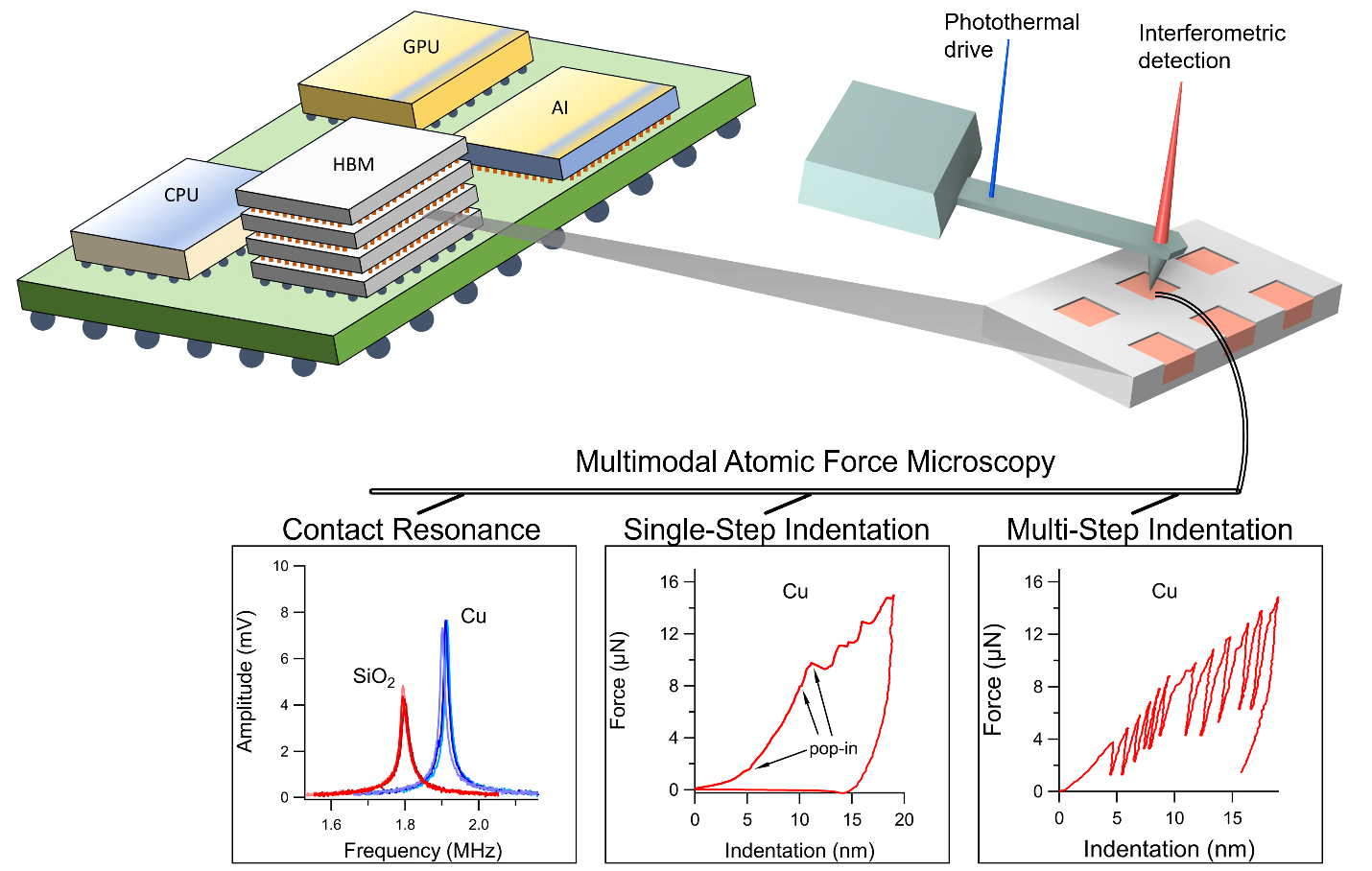
A mean flatness value can conceal local topography that prevents individual pads or dielectric regions from contacting. Metrology should therefore connect wafer-scale shape, site-level roughness, pad height, particle detection, alignment error, and post-bond void inspection to electrical results. Acceptance limits must be tied to a qualified downstream outcome, not chosen because an instrument can repeat them. When the process drifts, the evidence should identify whether surface preparation, placement, bonding, or anneal moved first.

NIST diagram connecting an advanced package and copper hybrid-bond pad to three atomic-force-microscopy measurement plots.

NIST links package geometry to nanoscale mechanical measurements of hybrid-bond-ready copper and dielectric surfaces.

The plots illustrate a research measurement method; production qualification still requires a broader process and reliability evidence set.The unmarked NIST diagram is public information with credit retained. It explains a research metrology method, not a production HBM stack or commercial bonding-line result.Gheorghe Stan / NIST.Original sourceNIST public information
A mechanically unstable package is an unreliable computer.

Spread 11 / Inspection, test, and qualification

11 / Verification

Find defects at the cheapest informative stage

Inspection sees structures; electrical test exercises behavior; reliability testing probes whether both endure.

Packaging test is layered because no single method reveals every failure. Optical and X-ray inspection can find alignment errors, cracks, voids, or missing features. Electrical tests check continuity, leakage, memory behavior, high-speed links, and power response. Thermal tests expose marginal joints or cooling paths. Burn-in and stress screens attempt to precipitate early failures before a module enters an expensive system.

Test coverage has a cost in equipment time, fixtures, data analysis, and sometimes product stress. Too little coverage allows escapes; too much poorly targeted testing slows output without improving field reliability. Engineers use failure analysis and process-control data to update screens and recipes. That feedback loop is central to yield learning: test is not only a gate at the end, but a sensor network for the entire assembly process.

Evidence ladder
  1. Inspect— Observe dimensions, surfaces, placement, and internal structures.
  2. Exercise— Test electrical functions and high-speed interfaces.
  3. Stress— Apply thermal, power, and environmental conditions.
  4. Learn— Connect failures to lots, tools, materials, and recipes.
Test at the cheapest informative boundary
GateQuestionFailure cost if missed
Die sortIs the component worth integrating?Other good components may be stranded
Post-bondDid the new interface form correctly?Fault localization becomes ambiguous
Final packageDoes the assembled system meet limits?Board and machine integration are exposed
System stressDoes behavior remain stable under duty?Fleet failures and service interruption
The best test stage is early enough to act and complete enough to matter.

Qualification / Field behavior

Passing a test is not the same as proving a fleet

Qualification defines a bounded use case; field reliability depends on workload, cooling, maintenance, and population scale.

A qualification plan specifies temperatures, power cycles, humidity, mechanical loads, duration, sample size, and acceptable failure criteria. Results apply to the tested design, materials, manufacturing route, and operating envelope. Changes to a substrate, underfill, bonding recipe, or thermal interface may trigger partial or full requalification because the coupled stack has changed. This protects reliability but slows substitutions during shortages.

Once deployed, telemetry provides a different evidence base. Correctable errors, thermal excursions, link retraining, performance throttling, and replacement history can reveal weak populations that preproduction samples missed. Suppliers and operators need traceability plus agreed escalation paths to turn those signals into containment and corrective action. Reliability is therefore a lifecycle information system joining package records to module, rack, workload, and service history.

Do not collapse these states
  • Electrically functional at final test
  • Qualified for a stated operating envelope
  • Accepted by a system integrator
  • Stable under real fleet workloads
  • Repairable within operational service targets
Turn escapes into learning
  1. Contain— Identify affected lots, recipes, tools, materials, and destinations before evidence is mixed or lost.
  2. Localize— Combine electrical signatures, imaging, genealogy, environmental history, and destructive analysis to isolate the layer.
  3. Correct— Change the process or screen, then prove effectiveness under representative stress without creating excessive rejection or a different escape path.
Reliability evidence grows from lot records into fleet telemetry.
04

Capacity, resilience, and handoff

The package leaves the factory only after specialized capacity, policy exposure, qualification, and module interfaces align.

Spread 12 / Capacity is a matched set

12 / Bottlenecks

One missing step caps the whole flow

Logic dies, memory stacks, interposers, substrates, bonding tools, test capacity, and qualified materials must arrive in compatible ratios.

Advanced-package capacity cannot be summarized by one factory number. A line may have bonding tools but insufficient tested HBM; substrates may arrive without enough interposer output; final-test equipment may lag assembly; or qualified materials may constrain recipe changes. Product mix further complicates the picture because package sizes, stack counts, test durations, and yields consume capacity differently. Nominal starts and usable modules can diverge sharply.

A dependency map should therefore track matched capacity and conversion at each gate. It should distinguish installed tools from qualified production, name the product families a line can run, and show the lag between expansion, process learning, and customer acceptance. This approach makes bottlenecks legible without pretending that commercially sensitive utilization data are public. The important insight is structural: the minimum compatible output among coupled stages governs delivery.

Capacity ledger
  • Qualified logic and interface dies by performance bin
  • HBM stack output by generation and configuration
  • Interposer, bridge, redistribution, and substrate capability
  • Assembly-tool throughput adjusted for product mix and yield
  • Final-test, burn-in, failure-analysis, and rework capacity
Capacity is a matched-flow claim: Installed tools, qualified process capacity, scheduled output, good output, and customer-accepted output are different denominators. A defensible map names the unit and time period at every gate, distinguishes pilot from volume lines, and shows whether materials, substrates, HBM, logic, assembly, thermal hardware, or final test sets the minimum compatible flow. Supplier revenue, announced investment, and front-end wafer capacity cannot substitute for packaging throughput when the latter is undisclosed.
The scarcest compatible stage sets qualified output.

Geography / Policy

The route crosses technical and legal borders

Specialized clusters create efficiency and expertise while exposing the assembly flow to trade, logistics, and policy changes.

Semiconductor design, wafer fabrication, memory production, substrates, assembly, and equipment are concentrated in specialized regional ecosystems. A component may cross borders several times as value accumulates. That route depends on freight capacity, customs classification, export licenses, secure data exchange, service access, and the ability of engineers to work across sites. A disruption can affect effective output without damaging a factory.

Export controls are especially time-sensitive. They may apply to equipment, technology, software, components, destinations, end users, or end uses, and their details can change faster than manufacturing footprints. An atlas should label current legal status and verification dates rather than infer unrestricted availability from physical capacity. Resilience can involve geographic diversification, inventory, alternate routing, dual qualification, or design flexibility, each with cost and learning tradeoffs.

Policy boundary: This volume maps dependencies, not legal entitlements. Operational decisions require current rules, license conditions, end-use screening, and counsel.
Actor map without false precision
  • Separate memory fabrication, logic fabrication, substrate production, assembly, equipment, materials, test, and system qualification; one company may occupy several roles.
  • Record geography at the facility and process-step level because corporate headquarters do not reveal where a qualified handoff occurs.
  • Use audited revenue and public awards as scoped financial signals, while stating when package-specific revenue, utilization, yield, or capacity is not disclosed.
Installed capacity and legally reachable capacity are different measures.

Spread 13 / Qualification and change control

13 / Substitution

A substitute must be re-proven inside the stack

Equivalent on a datasheet does not guarantee equivalent behavior after bonding, heating, loading, and years of operation.

Supply-chain resilience often calls for second sources, but advanced packages make substitution difficult. A new substrate vendor may use different process windows; an underfill may alter stress and heat transfer; a memory stack may share capacity and bandwidth while presenting different power or training behavior. The product must be evaluated at the interfaces where those differences matter rather than approved by category name alone.

Change control formalizes that work. Suppliers disclose changes, engineering teams assess risk, test vehicles isolate mechanisms, and qualification plans cover affected failure modes. The process can consume scarce samples and equipment, yet bypassing it transfers uncertainty into the fleet. Design-for-second-source begins early: tolerances, interfaces, telemetry, and validation hooks can preserve options that are almost impossible to add after production ramps.

Controlled substitution
  1. Identify— Define the exact material, process, or supplier change.
  2. Bound— Map electrical, thermal, mechanical, and reliability effects.
  3. Test— Use vehicles and product samples against stated criteria.
  4. Release— Approve, trace, monitor, and retain rollback information.
Qualify a substitution through the stack
  1. Declare— Describe the proposed material, supplier, process, tool, site, or design change and its intended benefit.
  2. Bound impact— Map interfaces, models, recipes, tests, reliability mechanisms, software assumptions, and customers that may be affected.
  3. Compare— Run controlled builds against the released baseline using predeclared acceptance limits and representative stress.
  4. Release— Approve, restrict, or reject the change while preserving evidence, genealogy, rollback, and notification requirements.
Resilience is designed through interfaces and evidence.

Learning / Ramp

Yield ramps are information ramps

Production improves when inspection, test, equipment, materials, and failure analysis resolve the causes behind loss.

Early production often reveals interactions that prototypes and simulations did not fully capture. Engineers classify defects, compare tools and lots, inspect cross-sections, model stress, and update recipes or design rules. The most useful metric is not only yield level but the pace and durability of learning: whether fixes address root causes, transfer across lines, and remain stable as volume and supplier mix change.

Data quality governs this process. Lot genealogy must connect dies, stacks, substrates, materials, tools, operators, tests, and downstream modules. Poor traceability turns a localized issue into broad containment because teams cannot identify the affected population. Conversely, telemetry without disciplined causal analysis can lead to false confidence. A mature ramp joins statistical process control with physical failure mechanisms and field evidence.

Operational insight: More tools increase nominal capacity. Better learning converts that capacity into repeatable, qualified assemblies.
Yield learning needs stable definitions
SignalMisreading to avoid
First-pass yieldCalling reworked output equivalent without tracking extra cycle time
Final yieldHiding which operation created or detected the defect
Test falloutAssuming every rejection represents a true product failure
Field returnComparing rates across fleets with different age or duty cycles
Ramp improvementCrediting learning while product mix or limits also changed
The ramp is complete only when output and evidence are both stable.

Spread 14 / From package to module

14 / Interface contract

The package hands constraints to the machine

Pinout, power rails, firmware, topology, thermal limits, mechanics, and test behavior become inputs to board and server design.

A qualified package is still not a deployable accelerator. Module designers must route host and scale-up links, place voltage regulation, connect management buses, provide clocking, secure the package mechanically, and establish a cooling interface. Firmware must initialize memory and links, expose sensors, record errors, and support recovery. Board tests then verify interactions that package test cannot reproduce fully.

The handoff should be treated as a controlled contract. It includes electrical models, thermal maps, keep-out zones, clamping limits, power sequences, firmware compatibility, error semantics, service instructions, and traceability identifiers. Any ambiguity becomes integration time or field risk. The next volume follows these packaged components into heterogeneous nodes, trays, power shelves, coolant manifolds, and rack-scale machines.

What crosses the boundary
  • Electrical interface and signal-integrity models
  • Rated, transient, and sequencing power requirements
  • Thermal map, sensors, pressure, and flatness limits
  • Firmware, diagnostics, error reporting, and security state
  • Handling, installation, removal, and failure-analysis rules
The package-to-machine interface contract
EnvelopeAcceptance evidence
ElectricalRails, sequencing, transients, telemetry, and fault response
ThermalPower map, limits, interface condition, mounting load, and sensor correlation
MechanicalKeep-outs, mass, flatness, retention, shock, vibration, and handling
LogicalIdentity, firmware, topology, reset, repair state, and diagnostic access
ReliabilityQualified stresses, use conditions, life assumptions, and escalation criteria
A package specification is a machine-design input.

Synthesis / Package

The completed assembly carries the upstream world

Inside one module sit minerals, chemicals, fabs, memory lines, integration tools, software contracts, and policy exposure.

Packaging condenses the intelligence buildout into a small physical volume. The assembly embodies wafer yields, memory-stack output, substrate chemistry, precision bonding, global logistics, engineering labor, and capital tied up across months of work. Its bandwidth and thermals influence how many accelerators a model needs; its reliability influences spares and maintenance; its power envelope influences racks and facilities.

The key analytical move is to resist treating packaging as an afterthought or memory as a commodity pool. Both are performance technologies and capacity systems. Their constraints propagate outward: fewer qualified packages limit server output, thermal limits shape liquid cooling, and memory placement shapes network traffic. The package is where fabricated parts become a computing promise. The machine is where that promise is tested under power, software, and service.

Dependency handoff: The next unit of analysis is the serviceable machine: accelerator modules plus hosts, links, power conversion, controls, cooling hardware, and rack mechanics.
Release the envelope, not just the part: A machine integrator needs the limits and evidence that make a package operable: mounting sequence, thermal-interface requirements, power excursions, supported firmware, error semantics, health counters, handling controls, and known restrictions. Acceptance should replay worst credible combinations rather than isolated maxima, because peak current, high inlet temperature, communication load, and mechanical tolerance can interact. A passing package test is necessary; a stable node under representative duty is the next proof boundary.
Package yield becomes machine availability only after another integration layer.

Behind the claim

Evidence, in context.

Opening the evidence record…